-
Products related to categories: servo, frequency conversion, HMI, driver, distributed DCS, IPC (PC bus industrial computer), PLC (programmable control system), DCS (distributed control system), FCS (field bus system), robot and other products and technical services.
-
Applications: Wind energy, automobile, ship, transportation, manufacturing, aviation, petroleum, natural gas, thermal power, thermal power, nuclear energy, steel, metallurgy, mining, power and other industries
-
Controller PLC\Robot servo drive Electro-hydraulic servo valve\DCS system/Distributed control systemSystem rack\Communication adapter\Analog output\Analog input\
-
\Multi-meter energy meter\Ignition\circuit board\Crimp terminal\Electric ac drive\Low voltage DC power module\Electro-hydraulic\servo valve\Automatic control system\exchange\Network communication module
controller\Processor module\dynamo\Electric machine\Servo drive\Touch screen\Input/output module\Water treatment monitoring system\Automobile\manufacturing system\Thermoelectric control system\ -
Digital output\Digital input\Mechanical protection system\High speed CPU
-
Electric power system\Chemical testing system\Petroleum control system\Tension monitoring system
-
DCS Distributed\control system\Steel control system\Steam\turbine system\Power generation system\
-
Thermal power generation system\Wind power system\Medium and high voltage frequency\conversion system\Precision motion system\Programmable control system\
-
Singapore New Energy Corporation
-
Geylang Bahru Industrial Estate
-
การทางหลวงแห่งประเทศไทย
-
American Petroleum Group
-
Indian shipping works
-
Pakistan Gas Company
-
Russian Automotive Industry Corporation
-
Brazilian Mining Company
-
Bangladesh Hydro power Plant
-
Egyptian Iron and Steel Manufacturing Co
-
Groupe d’exploitation du métro français
-
Für meinen vater
-
Mongolia Wind Farm
-
Empresa venezolana de procesamiento de petróleo
-
alibaba
-
Sichuan Huayingshan Power Plant
-
Huadian Datong Power Plant
-
Guodian Shuangyashan Power Generation Co., Ltd.
-
Baosteel Group Xinjiang Bayi Steel Co., Ltd.
-
Guodian Changzhou Power Plant
-
Xingtai Iron and Steel Co., Ltd.
-
Guodian Fee County Power Generation Co., Ltd.
-
Yangzhou Second Power Plant
-
Sichuan Jintang Power Plant
-
Xingcheng Special Steel Co., Ltd.
-
Quzhou Yuanli Metal Products Co., Ltd.
-
Zijin Mining Group
-
(Bangladesh) Metro Construction Company
-
WuHan steel co., ltd.
-
MaAnShan steel co., ltd.
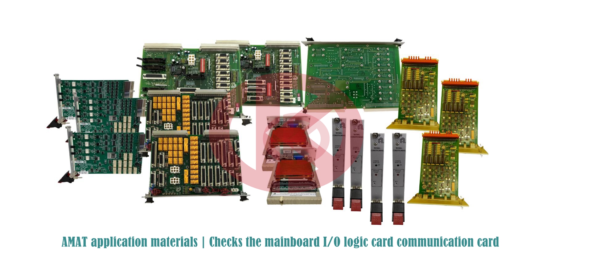
AMAT Applied Materials Company profile

AMAT Founded in 1967, Applied Materials is the world's largest nanomanufacturing technology company and the largest supplier of equipment, services and software products to the electronics industry.
The company has set up production, sales and service organizations in 13 countries and regions around the world, and is committed to promoting the development of global nanotechnology with high-tech equipment.
The company is headquartered in Santa Clara, California, USA. Applied Materials entered China in 1984 and now has offices or warehouses in Shanghai, Beijing, Tianjin, Suzhou, Wuxi and a solar energy development center in Xi 'an. In September 1993, Taiwan Applied Materials Co., Ltd.
was established in Taiwan to serve many semiconductor industry customers in Taiwan.
On May 21, 2018, the 2018 Fortune 500 list was released, and Applied Materials ranked No. 201.
Applied Materials' main products are related to chip manufacturing, such as atomic layer deposition, physical vapor deposition, chemical vapor deposition, electroplating, erosion, ion implantation, rapid heat treatment, chemical mechanical polishing, metrology and silicon wafer inspection. Applied Materials spends about $1 billion a year on research.
0200-00672
0190-14502
0100-71267
0190-15779
0021-84842
COMPONENT SIDE
0010-23715
0010-23716
went public on NASDAQ in 1972, and its stock code is AMAT.
Business Scope: The company operates through three main departments. The Semiconductor Systems department mainly provides capital equipment for semiconductor - chip manufacturing. The Applied Global Services department offers integrated solutions to optimize the performance and productivity of equipment and fabs, including spare parts, upgrades, services, remanufacturing of some old - equipment, and factory automation software for semiconductors, displays, and solar products. The Displays and Adjacent Markets department is engaged in products for manufacturing liquid - crystal and organic light - emitting diode (OLED) displays, as well as other display technologies and equipment upgrades for TVs, monitors, laptops, personal computers, tablets, smartphones, and other consumer - oriented devices.
Technological Edge: AMAT is a pacesetter in the fields of ion etching and thin - film deposition. Its products account for nearly 55% of the global PVD (Physical Vapor Deposition) equipment market share and about 30% of the global CVD (Chemical Vapor Deposition) equipment market share.
Market Position: AMAT is the world's largest semiconductor equipment company (except for lithography machines). It is recognized as one of the top - level global semiconductor equipment enterprises, along with Tokyo Electron (TEL) of Japan, ASML of the Netherlands, Lam Research (LAM) of the United States, and KLA of the United States. In 2023, its global market share of WFE (Wafer Fabrication Equipment) ranked second in the world, reaching 25%, and it ranked first in the world in terms of the number of products sold.
Company Scale: With approximately 24,000 employees worldwide, the company has more than 110 branches in 19 countries and regions. In 2024, its revenue was 26.52 billion US dollars, and its R & D investment was 3.1 billion US dollars.
- AEROTECH
- MOOG
- ABB
- HIMA
- GE
- Prosoft
- EMESRON
- EPRO
- rockwell
- Technical Data
- Product Information
- Industry Information
- Company News
- DEIF
- Triconex
- UNIOP
- REXROTH
- Woodward
- Lumentum
- Honeywell
- National Instruments
- Bently Nevada
- MOTOROLA
- FOXBORO
- Enterasys
- KOLLMORGEN
- SIEMENS
- SST
- YOKOGAWA
- sieger
- RELIANCE
- meggitt
- VMIC
- ALSTOM
- EATON
- METSO
- Abaco
- HIRSCHMANN
- Rolls-Royce
- BENDER
- AMAT
- Brand
- ORMEC
- WATLOW
- Schneider
- PRAXIS-Automation
- BASLER
- Kongsberg
- DISCO Corporation
-
ABB NINT-73C Drive control mainboard NINT73C 64425579A
-
BASLER DECS-250-CN1SN1N Digital Excitation Control System DECS250CN1SN1N
-
GE IS420ESWAH3A 8-port 10/100 base copper only
-
IS420ESWAH1A 8-port 10/100 base copper with one 100 Mbps
-
GE IS420ESWAH2A 8-port 10/100 base copper
-
GE IS420ESWBH1A 16-port 10/100 base copper with
-
GE PQMII-T20-C-A Power Quality Meter
-
GE Mark VI IS230PCAAH1A/B Combination module unit
-
ABB 3BHE021887R0101 UBCC717BE101 Board 3BHB002751R0102
-
ABB 3BHE032593R0001 Isolated Power Supply
-
ABB 3BSC610023R0001 POWER SUPPLY SD812
-
Sleeve matching ABB PFSC230 3BSE081054R1, 25M
-
ALSTOM 029.204431 Power unit module Accessory Mainboard
-
ALSTOM Converteam 029.302250 Power unit module
-
GE IS420UCSBH1A Mark Vle UCSC Controller
-
GE EX2100e Power Conversion Module 151X1235DB15SA1
-
MOOG G122‑829A P-I SERVO AMPLIFIER
-
S-D4017 Remote IO Backplane SSBP-1 RELIANCE drive module
-
CC-link card CCLK-1 S-D4030 RELIANCE drive module
-
Digital IO card DIO-1 S-D4006 RELIANCE drive module
-
S-D4041 DSPM-2A DSP RELIANCE drive module
-
abb 3BUS208720-001 POWER SIGNAL INTERCONNECT
-
GE DS3800NB1A Control Drive Board Serial Port Terminal Board
-
ABB EI813F 3BDH000022R1 communication card
-
TMEIC KPAD-3122A A3XAP02 LCD Display With Key Drive Accessories
-
ALSTOM F425368001 Rupture Disc 110 kV Gas Insulated Switchgear
-
80190-219-01G Allen Bradley Driver Pcb Board IGCT
-
GE DS3815PAHB1A Control Unit Drive Board
-
GE Mark VI IS230JPDGH1B Combination module unit
-
ABB 1MRK002247-Apr04 I/O-modules 670 series
-
ABB 0769143 A CELL SAMPLE AL175MM Gas analyzer accessories
-
RS NX700 Series Controller OEMAX SAMSUNG NX-Y64T
-
RS NX700 Series Controller OEMAX SAMSUNG NX-Y32T
-
NX700 Series Controller OEMAX SAMSUNG NX-X64D 64 output
-
NX-X32D 32 output Series Controller OEMAX
-
NX700 Series Controller OEMAX SAMSUNG NX-POSI4
-
NX-MWLINK Series Controller OEMAX SAMSUNG
-
RS NX-ETHERNET Series Controller OEMAX SAMSUNG
-
NX700 Series Controller OEMAX SAMSUNG NX-DEVICE
-
a-b NX700 Series Controller OEMAX SAMSUNG NX-CPU760C
-
NX700 Series Controller OEMAX SAMSUNG NX-BASE12
-
RS NX700 Series Controller OEMAX SAMSUNG NX-AO4V
-
NX700 Series Controller OEMAX SAMSUNG NX-AI8V
-
PowerFlex® 7000 ForGe Drives which utilize the new HMI Interface Board 80190-780-01-R
-
GCU-08 CB-130 80173-109-01-3 Mitsubishi Thyristor Inverter Power Board
-
a-b 1769-L30 CompactLogix 5370 L3 Controllers
-
A-B MicroLogix™ 1762-OW16 Relay Output Module
-
A-B 1761-ENT-AIC advanced interface converter
-
1761-CBC-PM02 ControlLogix Redundancy System cable
-
A-B 1746-IV16 16DI 10-30V DC SOURCE MODULE SLC 16 Digital Inputs
-
A-B 1746-IB16 module Rockwell SLC 16-point digital input control
-
A-B 1734-MB Memory system memory card
-
A-B 1336-BDB-SP4D 74103-244-54 1336 PLUS II Servo drive power board
-
RELIANCE 0-60067-1 0-60067 Automax Drive Board 0-60067-A
-
RELIANCE 0-60066-1 0-60066 S0-60066 Automax Drive Board
-
Meggitt C327845-11 Flow shutoff valve -7 -5 Parker
-
Driver board 029.204 686 Alstom power unit
-
ABB 3BSE020828R1 DSAI130DK01 Combined analog input module
-
ABB SCC-C 23070-0-101142100000 Continuous Emission Monitoring System (CEMS) Sample gas cooler
-
Siemens 6SE7038-6EK84-1JC2 Inverter Gate Triggering IGD8
-
GE IS200AEPBH1BBA Fan power generation power board
-
ALSTOOM MVS3000-4001 Handheld controller unit
-
PILZ 630613 PSEN OP 4H-S-30-060 Light Curtain Receiver
-
schneider SQUARE D POWERLOGIC CM4250 CIRCUIT MONITOR 96ma
-
EATON E84BAN Crane Control Heavy Duty Mill Limit Switch 2200 VAC 2NO-1NC Contact
-
MVI56 PDP-MV1 ALEN-BRADLEY PROSOFT PROFIBUS UNIT MVI56PDPMV1
-
ABB SCC-C Sample gas cooler 23070-0-10211110
-
GE PN.246B9953BPG1 TOOL-SCR REMOVAL
-
GUTOR BY SCHNEIDER ELECTRIC OP2446 MAIN PROCESSOR BOARD
-
HONEYWELL FX-USI-0002 Universal Safety Interface Module
-
HONEYWELL TA3840S Communication Unit
-
ABB 19P123085397 PDD AVR Unit
-
EMERSON 5X00899G01 Ovation™ Power Supply System
-
ABB 5SHY3545L0020 3BHE014105R0001 5SXE05-0154 IGCT Module
-
4TB5203-0402 Liquid crystal display panel
-
ABB 3BHE036348R0101 Expansion bracket card
-
ABB 3BHE017400R0101 PPD104 Extended memory card
-
ABB 3BHE012049R0001 Fiber Optic Expansion Motherboard
-
ABB 3BHE006805R0001 High Voltage Inverter Motherboard
-
ABB 3BHE000412R0101 INU INTERFACE BOARD
-
ABB UCD208A101 3BHE020018R0101 control board card
-
ABB 3ADT309600R0012 SDCS-CON-2 Terminal UNIT
-
80190-480-01-R Allen Bradley Driver Pcb Board
-
ABB DSMB179 57360001-MS MEMORYBOARD
-
ABB DSMB178 57360001-MM MEMORYBOARD CATALOG DESCRIPTION
-
ALSTOM C264MB1D69500130A300000C000N10 micom C264 ds agile bay controller
-
ABB PFSK138 3BSE014292R1 Channel Control Unit PFSK 138
-
GE ALSTOM 029.380 896 Board Logical control 029380896
-
ABB S-123H 3BHB030479R0112 Power unit ACS 6000 System
-
GE PLB029-376433 Phase-controlled control module of gas compression unit
-
GE IGBT ProX690-1E1-0L0H1 Phase-controlled control module of gas compression unit PLB029-370338
-
GE Industrial System Mark V Display MMI 323A2374P2
-
VMEBUS RACK VME32 BACKPLANE 100-240V/50-60 Hz/1200W
-
IBA ibaLink-SM-128V-i-2oVMEbus Interface Board SM128V
-
VMIC VME-PMC-CADDY VME-Carrier Board for 2 PMC Modules
-
ABB REF620E_1G Feeder Protection and Control
-
ABB SACO16D1 Digital Annunciator Unit
-
ABB REF620 HBFNACNNNEA1BNN11G Feeder Protection and Control
-
GE UT150-2 CPU MODULE CARD FOR CE2000 CONTROLLER
-
ALSTOM TANSFORMER MAINTENANCE KIT 1000KVA UTHC GEC
-
ABB DASD146 3ASC25H270 Lifter controller accessories DASD145
-
ABB DASD147 3ASC25H280 Lifter controller accessories DASD107
-
ABB SCC-K Converter NO2/NO converter and Thermal converter 3KXG801000U0100
-
Siemens 6AV6643-0CD01-1AX1 SIMATIC MP 277 10" Touch
-
ABB UAC095AE01 HIEE300788R0001 Communication Control IO Board
-
ABB AC800PEC Measuring Interface PECMIUAD140 PECMI UA D140
-
ABB 500PSM03 1MRB150038 Power Supply module
-
Valmet metso D201563L Control unit accessories
-
Valmet metso D201473L AII8 Control unit accessories
-
EATON XVS-430-10MPI-1-10 Touch panel 24 V DC TFTcolor, ethernet, RS232
-
bently 60M100-00 Condition Monitoring System
-
ABB 3BHB004791R0101 IGCT Gate Power Supply Unit
-
ABB TAS.580.0550.G00 HARDWARE BOARD ABB100 COMPONENTS SIDE
-
ABB SYN5201A-Z,V277 3BHB006714R0277 Automatic single-channel synchronization unit
-
ABB SUE3000 1VCF750090R0804 Operation screen unit 1VCR007346
-
ABB SENSYCAL FCU400-IR Product Summary
-
ABB SDCS-CON-2-COAAT 3ADT220090R2 DCS Thyristor Power Converters accessories
-
ABB SCYC51220 63901075c Control Module
-
Siemens SYNCHRONOUS SERVOMOTOR 1FK6084-6AZ21-9ZZ9-Z S05
-
Siemens SYNCHRONOUS SERVOMOTOR 1FK6063-6AF71-1EH0
-
FOXBORO FBM241/b/c/d Discrete I/O Interface Modules
-
FOXBORO FBM242, Externally Sourced, Discrete Output Interface Module
-
FOXBORO FBM244, 0 to 20 mA I/O Interface Module with HART Support
-
FOXBORO FBM245, 0 to 20 mA I/O Interface Module with HART Support
-
FOXBORO FBM247, Current/Voltage Analog/Digital/Pulse I/O Configurable Interface Module
-
FOXBORO FBM218 HART Communication Redundant Output Interface Module
-
FOXBORO FBM219 Discrete I/O Interface Module
-
FOXBORO FBM222, Redundant PROFIBUS Communication Interface Module


All new products and surplus products of the industrial intelligence industry, as well as the discontinued products of the original manufacturers. We are not an authorized distributor or representative of any of the above manufacturers (except for brand authorization). The trademarks, brand names and brands appearing in this agreement are the property of their respective manufacturers.
COPYRIGHT© 2003-2026 Copyrighted

Phone(WeChat/Whatsapp)
+086-181 4410 0983
No 1134 Jimei North Road,
Hong Kong Office:
Guan Tang District, Hong Kong,
